- 您现在的位置:买卖IC网 > Sheet目录2007 > LTC6991MPS6#TRPBF (Linear Technology)IC OSCILLATOR RESET LF TSOT23-6
LTC6991
9
6991fb
OPERATION
The LTC6991 is built around a master oscillator with a
1MHz maximum frequency. The oscillator is controlled
by the SET pin current (ISET) and voltage (VSET), with a
1MHz 50k conversion factor that is accurate to ±0.8%
under typical conditions.
fMASTER =
1
tMASTER
= 1MHz 50kΩ
ISET
VSET
A feedback loop maintains VSET at 1V ±30mV, leaving ISET
as the primary means of controlling the output frequency.
The simplest way to generate ISET is to connect a resistor
(RSET) between SET and GND, such that ISET = VSET/RSET.
The master oscillator equation reduces to:
fMASTER =
1
tMASTER
=
1MHz 50k
Ω
RSET
From this equation, it is clear that VSET drift will not affect
the output frequency when using a single program resistor
(RSET). Error sources are limited to RSET tolerance and
the inherent frequency accuracy ΔfOUT of the LTC6991.
RSET may range from 50k to 800k (equivalent to ISET
between 1.25μA and 20μA).
Before reaching the OUT pin, the oscillator frequency
passes through a fixed ÷1024 divider. The LTC6991 also
includes a programmable frequency divider which can
further divide the frequency by 1, 8, 64, 512, 4096, 215,
218 or 221. The divider ratio NDIV is set by a resistor divider
attached to the DIV pin.
fOUT =
1MHz 50k
Ω
1024 NDIV
ISET
VSET
, or
tOUT =
1
fOUT
=
NDIV
50k
Ω
VSET
ISET
1.024ms
with RSET in place of VSET/ISET the equation reduces to:
tOUT =
NDIV RSET
50k
Ω
1.024ms
DIVCODE
The DIV pin connects to an internal, V+ referenced 4-bit A/D
converter that determines the DIVCODE value. DIVCODE
programs two settings on the LTC6991:
1. DIVCODE determines the output frequency divider set-
ting, NDIV.
2. DIVCODE determines the polarity of the RST and OUT
pins, via the POL bit.
VDIV may be generated by a resistor divider between V+
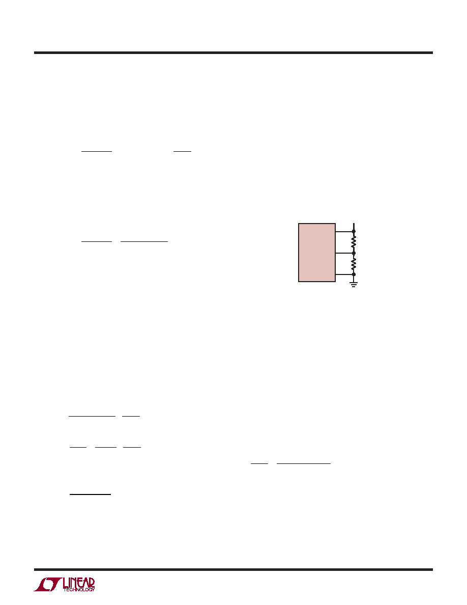
and GND as shown in Figure 1.
Figure 1. Simple Technique for Setting DIVCODE
6991 F01
LTC6991
V+
DIV
GND
R1
R2
2.25V TO 5.5V
Table 1 offers recommended 1% resistor values that ac-
curately produce the correct voltage division as well as the
corresponding NDIV and POL values for the recommended
resistor pairs. Other values may be used as long as:
1. The VDIV/V+ ratio is accurate to ±1.5% (including resis-
tor tolerances and temperature effects)
2. The driving impedance (R1||R2) does not exceed 500kΩ.
If the voltage is generated by other means (i.e., the output
of a DAC) it must track the V+ supply voltage. The last
column in Table 1 shows the ideal ratio of VDIV to the
supply voltage, which can also be calculated as:
VDIV
V+
=
DIVCODE
+0.5
16
±1.5%
For example, if the supply is 3.3V and the desired DIVCODE
is 4, VDIV = 0.281 3.3V = 928mV ± 50mV.
Figure 2 illustrates the information in Table 1, showing
that NDIV is symmetric around the DIVCODE midpoint.
发布紧急采购,3分钟左右您将得到回复。
相关PDF资料
LTC6992MPS6-4#TRPBF
IC OSC PWM VOLT CTLR TSOT23-6
LTC6994CDCB-2#TRPBF
IC DELAY LINE 6-DFN
LTC7541ABN#PBF
IC CMOS D/A CONV 12BIT 18-DIP
LTC7545ACG#TRPBF
IC D/ACONV MULTIPLY 12BIT 20SSOP
LTC8043EN8
IC D/A CONV 12BIT SERIAL 8-DIP
LTC8143ESW#TRPBF
IC D/A CONV 12BIT SERIAL 16-SOIC
LTM9011CY-14#PBF
IC ADC 14BIT UMODULE 140BGA
LV5609LP-E
IC CLOCK DRIVER VERTICAL 24VCT
相关代理商/技术参数
LTC6992-1
制造商:LINER 制造商全称:Linear Technology 功能描述:TimerBlox Voltage-Controlled Pulse Width Modulator (PWM)
LTC6992-2
制造商:LINER 制造商全称:Linear Technology 功能描述:TimerBlox Voltage-Controlled Pulse Width Modulator (PWM)
LTC6992-3
制造商:LINER 制造商全称:Linear Technology 功能描述:TimerBlox Voltage-Controlled Pulse Width Modulator (PWM)
LTC6992-4
制造商:LINER 制造商全称:Linear Technology 功能描述:TimerBlox Voltage-Controlled Pulse Width Modulator (PWM)
LTC6992CDCB-1#PBF
制造商:Linear Technology 功能描述:SC-Timing, Cut Tape PWM with 0% to 100% Pulse Width Control
LTC6992CDCB-1#TRMPBF
功能描述:IC OSC SILICON 1MHZ 6-DFN RoHS:是 类别:集成电路 (IC) >> 时钟/计时 - 可编程计时器和振荡器 系列:TimerBlox® 标准包装:3,000 系列:- 类型:振荡器 - 晶体 计数:- 频率:- 电源电压:2.3 V ~ 5.5 V 电流 - 电源:1.07mA 工作温度:-30°C ~ 80°C 封装/外壳:SOT-665 包装:带卷 (TR) 供应商设备封装:SS迷你型-5D 安装类型:表面贴装 其它名称:AN8955SSMTXLTR
LTC6992CDCB-1#TRPBF
功能描述:IC OSC SILICON 1MHZ 6-DFN RoHS:是 类别:集成电路 (IC) >> 时钟/计时 - 可编程计时器和振荡器 系列:TimerBlox® 产品培训模块:Lead (SnPb) Finish for COTS
Obsolescence Mitigation Program 标准包装:45 系列:- 类型:温度 - 补偿晶体振荡器(TCXO) 计数:- 频率:25MHz 电源电压:3.135 V ~ 3.465 V 电流 - 电源:1.5mA 工作温度:-40°C ~ 85°C 封装/外壳:16-SOIC(0.295",7.50mm 宽) 包装:管件 供应商设备封装:16-SOIC W 安装类型:表面贴装
LTC6992CDCB-1TRMPBF
制造商:Linear Technology 功能描述:PWM Voltage Controlled 3.81Hz-1MHz DFN6